


BMP TO ASCII TOOL Directions 把圖形轉換成ASC檔案
BMP TO ASCII TOOL Directions.
This tool was written by J
ames Tidman (jtidman@flash.net) and was originally available from
http://www.flash.net/~jtidman/BMP2ASC/BMP2ASC.html
The file required is here.
Click Here for BMP2ASC.EXE
If your on the PADS ListServer you probably know Mike Poorman.
This link is just to embarrass him.
Mike Poorman as Product Tester
Here is a document I wrote on Embedding Drill tables in PADS PCB
embedding_drill_tables.doc
Here is a document Dave White of Mentor dave_white@mentorg.com gave me on comparing net lists with CAM350.
Netlist compare in CAM350 V8.pdf
Utility to Port PADS Netlest from ORCARD with full atributes from chuck.tidwell@silabs.com.
PowerNET_v2_0b03.zip
Why?
This tool is used to import company or regulatory logos, or other graphical elements into the PADS database. These images can then be placed on the silkscreen, or any other layer.
How?
This tool will scan a windows BMP (two color only) file and convert it into a PADS .ASC file format. This file can then be imported into the design database.
In scanning the BMP file, a left to right, top to bottom approach is used. Each continuous group of white pixels is translated into a single line segment in the ASC file.
What is the best method to use?
Any two color, black and white BMP file can be converted. However, for best results, please use the following method (we’ll talk in Mils, and try to show examples):
First, we need the image we need to convert the image to a size and format we can use.

This is the original Image. First we need to convert to 2 colors and make it a BMP (Windows BitMap File).
I would like to take this time to plug my favorite tool for the graphical work: PaintShop Pro. You can get it from http://www.jasc.com/.
This is a useful tool for grabbing images from the screen, converting them to black and white, scaling them to fit and saving them in windows bitmap format.
If using PSP use Colors / Decrease Color Depth / 2 colors. The image now looks like this.

Now Use Colors Negative Image to get this result.

Lastly save as a BMP file - if the file is very large you might want to scale it first.
When the image is imported the ration is 1 pixel = 2 mills. So if you want the image to be 500mills x 250mills draw it as 250x125 pixels.
I usually take what I get and use PADS to scale it as I need for the application.
Once this bit map is saved in 2 color mode, we run the program with the following arguments (assuming the program and the bit map are in the same directory):
BMP2ASC input.bmp output.asc 2 26 0 0
The format for this command is BMP2ASC .
This will scan the data and convert it to horizontal lines 2 mils wide.
These lines will be placed on layer 26 (silkscreen top), and the lower left-hand corner of the image will be at 0,0.
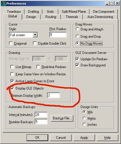
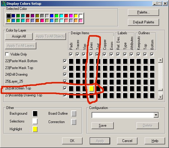
Next open up a new PADS file, and import the ASC file INTO AN EMPTY FILE (FILE/ NEW FILE/IMPORT/ASCII FILE). Be sure to set the color and the minimum display width: Also be sure that the silk layer is turned on (has a color assigned to it). You will probably want to hit "home" to find your image.
Select the complete item, and then combine it (Right Mouse Button - Select Anything - CTRL A - Right Mouse Button Combine).
This may take a while for complex images. Once complete, select save to library from the mouse right-click menu when in the drafting..
You can now past it in to existing designs using the paste from library button bar:
If it is not scaled the way you want you may change scale and layer. Example scale 2:1 and move to copper layer.
To Scale - place the image where you want.
RMB - SELECT SHAPE - (select shape) - RMB EXPLODE - RMB SCALE
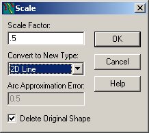
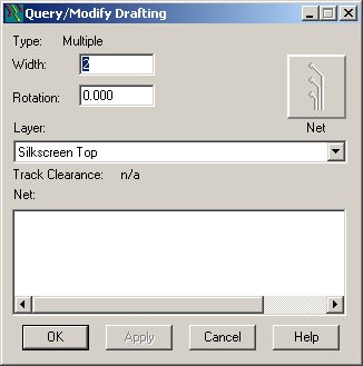
This example makes the output 1/2 the size of the original. Note the PADS scale command currently always puts 2d lines on the top layer. Next select the object - RMB Query Modify - change the layer back to silk (or where ever you want it).
Now RBM Combine and your done.
=============================================================
Embedding Drill Tables in PADS PCB and PADS output format setup.
PADS PCB has a rudimentary way to embed all drill information into the drill files it generates. This embedding is much like the difference between RS-274-D and RS-274-X with it’s embedded aperture tables.
Embedding drill tables saves steps in producing boards, removes the potential for errors, and improves verification ability of files before sending them for fabrication. For this reason I believe that Nexus Technologies should adopt this simple change.
To embed Drill Files in your .dll you need to follow a few simple set-up steps. Once these are done the first time PADS remembers this set up information and stores it.
The first part of this procedure explains how to set up for the embedded drill format. The second part shows set up for embedded Gerbers and proper output as well as other tips for better PADS generated Gerbers.
NC Drill Setup
1) Under CAM setup for drill files, under Format String, choose Drill File Start from the Type field. Change the String field from % to M48@n%. This provides a proper Excellon Start Header command, which was missing from the format.
2) In the same dialogue box, choose Tool Section Start from the Type field. Change the String field from the default of T@tF@fS@s to T@tC@dF@fS@s. This tells PADS to insert the following information into the drill table output
· T@t = Tool Number Table
· C@d = Tool Diameter (Size) Table
· F@f = Drill Feedrate (IPM) Table
· S@s = Drill Speed (SFPM) Speed
3) In addition please make sure that all other setting match the example above. Format should be Excellon, Absolute Coordinates, 3 leading, 5 trailing digits with Trailing Zero Suppression, English units.
4) Unfortunately, due to a bug in PADS 5.01 and before (which is scheduled to be fixed after the release of 5.2), you MUST change the preferences units from Mills to Inches before outputting the drill file. This means you must follow these steps.
· Set, in preferences
(Setup/Preferences), the design units to Mills.
· Output all Gerbers EXCEPT the drill file.
· Set, in preferences, the design units to Inches.
· Output the NC drill file.
· Return the design units to Mills.
5) Another handy NC drill and Drill Drawing program is called D3T_101.BAS. It is located at http://www.mindlinktech.com/Downloads/d3t.htm . This program was intended to output a drill table for DXF export, but it has another use.
It will clean up the drill table and order the drill pairs by size. To use this VB script output the Drill drawing, run the script, delete the generated drill table (on the PCB) and re-generate the, now ordered, drill table.
PADS Setup and Tips for Proper Gerber Outputs.
To Setup PADS PCB Gerber output set all fields in the Photo Plotter ADVANCED TAB as listed and shown below.
· Output format to RS-274-X (this embeds the Aperture Table) (This will change the number of apertures to 989)
· Number of digits to 3 leading and 5 trailing.
· Coordinates to Absolute.
· Zero Suppress to Leading
· Make sure Fill & Macro are all unchecked (due to issues with these formats with some Gerber Readers).
· Under the Photo Plotter Setup box make sure Augment on-the-fly is checked.
· You MUST regenerate all D-Codes before plotting Gerbers. This is due to a PADS bug that will cause all end-points to be drawn and not flashed.
Tip for plotting all Gerbers:
Under Plot Options do not use Center Justification. Instead use Offset and set all outputs, including NC drill outputs to a common offset such as 10000x1000. This ensures that all Gerbers properly line up when imported into the CAM software and prevents miss alignment and offset errors.
Another Tip for ensuring accurate Gerbers is to use the script IPC-D-356A_Netlist_Extractor.4_7_2_1.bas available from http://www.siliconhills.com/design_utilities.html .
This utility outputs an IPCD-356-A net-list from PADS.
This net-list is used for testing of bare boards. It is usually extracted from the Gerbers by the board house.
The advantage of extracting it from the PCB database over the Gerbers is that it will now also catch errors in the Gerber output.


沒有留言:
張貼留言