
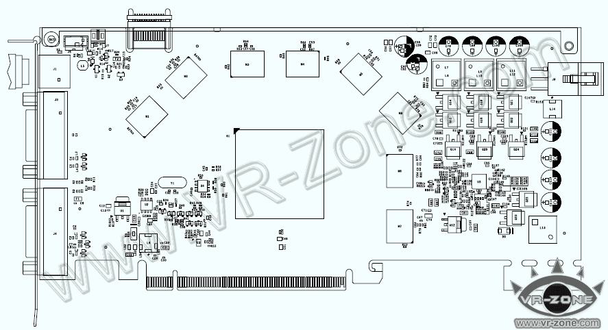
In the weeks to come, NVIDIA will release yet another graphics card based on the G92 graphics processor: the GeForce GTS 240, which bears resemblance with the 8800 GT and 9800 GT.
The G92 GPU has near-identical specifications to the said graphics cards, except for that the 55 nm G92b GPU will be used, and with higher reference clock speeds of 675/1674/975 MHz (core/shader/memory). To seat the new GPU, NVIDIA has designed a new reference PCB, the P361 internally called D10P2.
The schematic drawings of this has been sourced by VR-Zone.
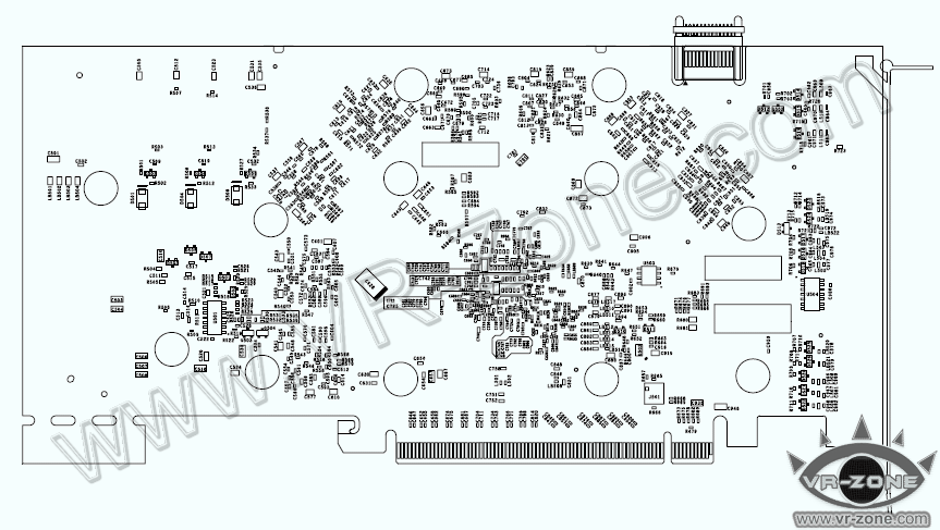
The P361 PCB covers the basics of accommodating the G92b and eight GDDR3 memory chips connected to the GPU across a 256-bit wide bus.
The P361 PCB covers the basics of accommodating the G92b and eight GDDR3 memory chips connected to the GPU across a 256-bit wide bus.
The distinct features of the PCB lie with its VRM area, with a 3+1 phase design. The PCB draws power from a 6-pin PCI-Express power connector.
Over to the connectors department, the usual two arrangement of two DVI and one composite is present.
There is a single SLI bridge connector for 2-way SLI. With the 55 nm GPU being arguably as cool or cooler than the 65 nm G92 with lower reference clock speeds, one can expect a single slot cooler design to be employed.
(↑點擊變大尺寸圖片~ZOOM+↑)
這是ALLEGRO PCB LAYOUT的板子,
大家可以參考看看!!
改天我再PO一個
有20個GDDR3的大型顯示卡給各位欣賞
哈哈...
真是很壯觀勒!!
Flyfish 2009.02.24 Pm17:22
沒有留言:
張貼留言